Thermal
radiative properties of nanostructures
The ability to manufacture, control, and manipulate
structures at extremely small scales is the hallmark of modern
technologies, which include microelectronics, MEMS/NEMS, and
nanobiotechnology. Spectral and directional control of thermal
radiation is a challenging yet important task for a number of
applications, such as thermophotovoltaic (TPV) energy conversion,
solar energy utilization, space thermal management, and
high-efficiency incandescent lamps. The key to the enhancement of
performance is through the modification of the reflection and
emission spectra using one-, two-, or three-dimensional
micro/nanostructures [1]. Pattern-induced radiative property
variations can be an important problem for the wafer temperature
measurement and the temperature uniformity control during integrated
circuit manufacturing. In addition, light diffraction can be used to
monitor the etching depth and other features during the
microfabrication and lithographic processes.
We have fabricated both 1-D and 2-D periodically
patterned microstructures using silicon microfabrication technology.
The bidirectional reflection was measured using the three-axis
automatic scatterometer, developed in our lab (see facilities).
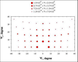
Figure 4 shows the bidirectional reflection of the 2-D
microstructured silicon surface. The grating period is 5
mm in both direction and
the wavelength is 535 mm.
There are 2.25 million square structures in a single sample of an
area of 7.5 ´ 7.5 mm2.
The differently sized circles in Fig. 4b indicate different ranges
of the power ratio, averaged over the two polarizations. The
diffraction pattern is symmetric with respect to
yx = 0°
and nearly symmetric along the diagonal. The angular locations of
the diffraction measurements are in excellent agreement with the
prediction. The result may serve as a benchmark for the validation
of 3-D rigorous electromagnetic wave models for 2-D microstructures.
|
 |
 |
|
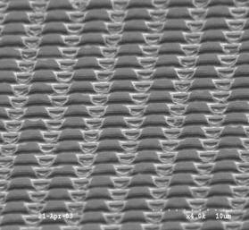
Figure 1. (a) SEM imaging of 2-D microfabricated structure
on silicon, and (b) the diffraction pattern at normal
incidence. |
In the flashlamp thermal processing, the heating cycle
is on the order of millisecond. It is very important to determine
the radiative properties of the patterned structures in order to
assess the thermal budget and temperature uniformity. We have
calculated the radiative properties of patterned wafers with the
smallest dimension down to 30 nm [3]. The effects of wavelength,
polarization, and angle of incidence on selected periodically
patterned wafers have been investigated. The rigorous coupled wave
analysis (RCWA) and two effective medium approaches (EMA-1 and
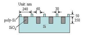
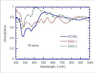
EMA-2) are used. Figure 2 shows the normal absorptance of the 1-D
patterned structure, shown on the left, for a TE wave, that is, the
electric field is parallel to the grooves. The absorptance is a
complicated function of wavelength due to the variation of the
dielectric function of silicon and the unique effect of gratings.
The use of EMA may result in a large error in the predicted
radiative properties [3]. Further research is needed to determine
the impact of the overall absorption on the wafer temperature
distribution.
 |
 |
|
Figure 2. Predicted reflectivity at normal incidence for
the structure shown on the left. |
In the future, complex grating structures will
be constructed using heavily doped silicon as wavelength
selective emitters and absorbers for radiative energy conversion
and thermal radiation detection. Particular attention will be
paid to the study of the near-field effect on the far-field
performance of these device structures. The radiative properties
of patterned waves will be measured and compared with the
prediction to assist the evaluation and development of very
short-time thermal manufacturing of semiconductor devices.
This work has been supported by the National Science
Foundation.
Selected Publications
[1] Zhang, Z.M., Fu, C.J., and Zhu,
Q.Z., 2003, "Optical and Thermal Radiative Properties of
Semiconductors Related to Micro/Nanotechnology," Advances in
Heat Transfer, 37, pp. 179-296.
[2] Chen, Y.B., Zhu, Q.Z., Wright, T.L.,
King, W.P., and Zhang, Z.M., 2004, "Bidirectional Resection
Measurements of Periodically Microstructured Silicon Surfaces,"
International Journal of Thermophysics, 25, pp.
1235-1252.
[3] Chen, Y.-B., Zhang, Z.M., and
Timans, P.J., 2005, "Radiative Properties of Patterned Wafers
with Linewidth below 100 nm," to be presented at the
International Mechanical Engineering Congress and Exposition,
November 5-11, 2005, Orlando, FL.
Go to TOP