Study of
the radiative properties of rough surfaces for temperature measurements in rapid
thermal processing
The
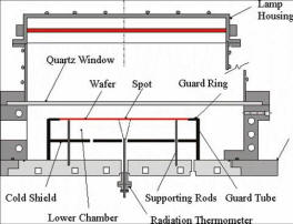
motivation of this research is to accurately measure the temperature of silicon
wafers using radiation thermometers during the rapid thermal processing (RTP),
see Fig. 1. RTP is a key technique for the advance of integrated circuits to
meet requirements towards the shrinkage of devices size and increasing packing
density. With advantages in temperature control, short cycle, and process
flexibility, RTP has expanded its application areas such as annealing for
surface damage removal, the growth of thin oxides or nitrides, chemical vapor
deposition, and so on. A challenging problem in the RTP technique is to
accurately measure the temperature of silicon wafers (refer to Fig. 1). Due to
fast response and non-intrusiveness, light-pipe radiation thermometers (LPRTs)
are frequently chosen to monitor the temperature of the wafer during processing.
However, in radiation thermometry, the variation in wafer emissivity and the
stray radiation from background significantly affect the measurement uncertainty
[1]. The monitored surface of silicon wafers
generally possesses roughness created by mechanical cutting and chemical
etching. Surface roughness alters not only the emissivity of silicon wafers but
also the effect of the background radiation by scattering the incident
radiation. In fact, the effective emissivity considering the effect of
background radiation is used in temperature reading with an LPRT instead of the
intrinsic emissivity. Therefore, understanding the directional dependence of
scattering from rough silicon surfaces is essential for radiometric temperature
measurement of silicon wafers during RTP.
|
 |
 |
|
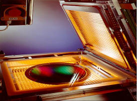
Figure 1.
A rapid thermal processing furnace and the temperature measurement of a
silicon wafer using the radiation thermometer. |
The bidirectional reflectance and transmittance
distribution functions (BRDF and BTDF) are fundamental radiative
properties that describe the re-distributions of radiative energy
after scattering from rough surfaces. Once the bidirectional
properties are known, the emissivity can be obtained from the
integration of them. However, a true importance of the bidirectional
properties lies in considering the effect of background radiation.
Because the background radiation originates from multiple
reflections between silicon wafer and an RTP chamber, knowledge of
the bidirectional properties enables to model the effective
emissivity [2].
We
started this research by modeling the effective emissivity in an RTP furnace
with the net-radiation method [3] and the Monte Carlo method [4], based on
specular/diffuse reflection assumptions. At the same time, we made an effort to
find appropriate analytical models for the BRDF of silicon wafers using the
reference optical scatterometer at the National Institute of Standards and
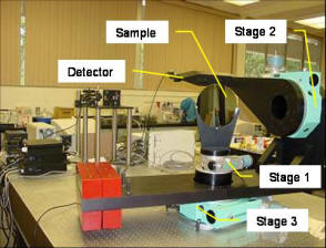
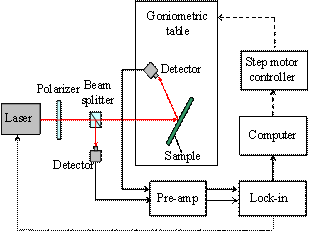
Technology (NIST) [5]. Subsequently, we developed a custom-designed optical
reflectometer, namely, three-axis automated scatterometer (TAAS), as shown in
Fig. 2 [6].
 |
 |
|
Figure 2. Picture and
schematic representation of TAAS. |
The
goniometric table composed of three rotary stages offers high angular resolution
and repeatability to determine the incidence and reflection directions and
allows us to measure both the BRDF and the BTDF in and out of the plane of
incidence with high accuracy. A compact diode laser system provides high
wavelength and power stabilization, and the fiber-coupled laser is easily
interchangeable for a different wavelength. A lock-in amplifier modulates the
power of the laser directly to avoid noises from the background radiation.
Highly linear diode detectors with transimpedance amplifiers provide a large
dynamic range. A reference detector eliminates the unnecessary sample moving and
enables fast sampling. The sample holder allows a large sample up to 8” diameter
to be measured. Heated sample compartment and additional translation and
rotation stages can be included in the system for the emissivity measurement and
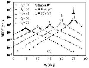
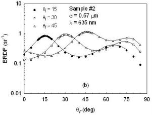
surface scan, respectively. Good agreement was obtained between the measured
results from TAAS and the reference instrument in NIST, as shown in Figure 3 for
two different silicon surfaces. The all-round capability of TAAS allowed
extensive studies of the bidirectional radiative properties.
 |
 |
|
Figure
3. Comparisons of measurement results from TAAS (solid line) and the
reference instrument in NIST (mark) for two different silicon
wafers. |
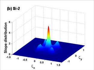
Because the statistics of surface roughness is essential for modeling
approaches, we measured the surface topography of a number of silicon wafers
with an atomic force microscope (AFM). While the height distribution function of
a silicon wafer is close to a Gaussian functional form, the slope distribution
function is anisotropic [7]. Consequently, a one-dimensional modeling approach
with the assumption of isotropic surfaces is not applicable to the BRDF of
silicon wafers. Figure 4 shows the slope distribution functions of two silicon
wafers. Note that Si-1 is slightly anisotropy whereas Si-2 is highly anisotropy
with side peaks. Further study demonstrated that the anisotropic orientation of
silicon surface roughness is caused by the chemical etching process. Using the
geometric optics based model, the BRDF can be correlated with the crystalline
structure of silicon at the microscale [8].
 |
 |
|
Figure
4. Anisotropic slope distribution of two silicon wafers obtained
from the measured surface topography using an atomic force
microscope. |
Meantime, we have developed a Monte Carlo method to predict the BRDF and BTDF
simultaneously and studied the variation of hemispherical properties under
various conditions [9]. This Monte Carlo method furthermore has a potential to
model the effective emissivity by employing the statistics of surface roughness
such as the root-mean-square (rms) roughness and autocorrelation length, without
relying on the analytical BRDF model. We continued to improve and extend the
Monte Carlo method for the radiative properties of rough surfaces with thin-film
coatings [10] and evaluated the applicability of the geometric optics
approximation with the Monte Carlo method [11]. Recently, the Monte Carlo method
is further developed to directly incorporate the two-dimensional surface
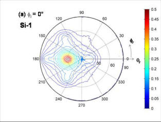
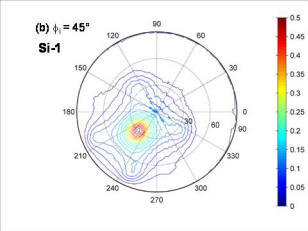
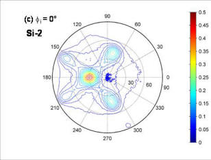
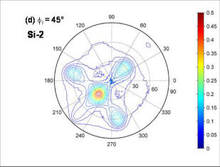
topography obtained from the AFM measurement. The predicted BRDFs of the
anisotropic silicon wafers, based on the measured surface topography, are
presented in Fig. 5, at 30º incidence angle and a wavelength of 635nm. The BRDFs
reveal the same anisotropic features as the slope distribution function shown in
Fig. 4b, implying that the effect of microroughness is significant to the
bidirectional radiative properties.
In future research, we will study thin-film coatings on the
bidirectional properties by coating the silicon surfaces with metallic and
dielectric coatings. The hemispherical radiative properties will be studied with
an integrating sphere, and a monochromatatic light source will be used to expand
the spectral range. In the long run, this research will not only gain a better
understanding of radiation heat transfer at the microscale but also benefit
semiconductor industry.
This work has been supported by the National Science Foundation
(CTS-0236831) and the National Institute of Standards and Technology (Optical
Technology Division).
Selected Publications
[1] Zhang, Z. M., "Surface Temperature Measurement
Using Optical Techniques," in Annual Review of Heat Transfer, vol. 11, C.
L. Tien, Ed. New York: Begell House, 2000, pp. 351-411.
[2] Zhang, Z. M., Fu, C. J., and Zhu, Q. Z., "Optical
and Thermal Radiative Properties of Semiconductors Related to
Micro/Nanotechnology," in Advances in Heat Transfer, vol. 37. New York:
Academic press, 2003, pp. 179-296.
[3] Zhang, Z. M., and Zhou, Y. H., 2001, "An Effective
Emissivity Model for Rapid Thermal Processing Using the Net-Radiation Method,"
International Journal of Thermophysics, 22, pp. 1563-1575.
[4] Zhou, Y. H., Shen, Y. J., Zhang, Z. M., Tsai, B.
K., and DeWitt, D. P., 2002, "A Monte Carlo Model for Predicting the Effective
Emissivity of the Silicon Wafer in Rapid Thermal Processing Furnaces,"
International Journal of Heat and Mass Transfer, 45, pp. 1945-1949.
[5] Shen, Y. J., Zhang, Z. M., Tsai, B. K., and
DeWitt, D. P., 2001, "Bidirectional Reflectance Distribution Function of Rough
Silicon Wafers," International Journal of Thermophysics, 22, pp.
1311-1326.
[6] Shen, Y. J., Zhu, Q. Z., and Zhang, Z. M., 2003,
"A Scatterometer for Measuring the Bidirectional Reflectance and Transmittance
of Semiconductor Wafers with Rough Surfaces," Review of Scientific Instruments,
74, pp. 4885-4892.
[7] Zhu, Q. Z., and Zhang, Z. M., 2004, "Anisotropic
Slope Distribution and Bidirectional Reflectance of a Rough Silicon Surface,"
Journal of Heat Transfer, 126, pp. 985-993.
[8] Zhu, Q. Z., and Zhang, Z. M., 2005, "Correlation
of Angle-Resolved Light Scattering with the Microfacet Orientation of Rough
Silicon Surfaces," Optical Engineering, 44, 073601.
[9] Zhou, Y. H., and Zhang, Z. M., 2003, "Radiative
Properties of Semitransparent Silicon Wafers with Rough Surfaces," Journal of
Heat Transfer, 125, pp. 462-470.
[10] Lee, H. J., Lee, B. J., and Zhang, Z. M., 2005,
"Modeling the Radiative Properties of Semitransparent Wafers with Rough Surfaces
and Thin-Film Coatings," Journal of Quantitative Spectroscopy and Radiative
Transfer, 93, pp. 185-194.
[11] Zhu, Q. Z., Lee, H. J., and Zhang, Z. M., 2005,
"The Validity of Using Thin-Film Optics in Modeling the Bidirectional
Reflectance of Coated Rough Surfaces," Journal of Thermophysics and Heat
Transfer, 19, in press.
Go to TOP