Coherent
thermal emission from modified periodic multilayer structures
Thermal radiation emitted from solids is generally manifested
by a broad spectrum and quasi-isotropic angular behavior. Coherent
thermal emission has drawn much attention lately for applications in
thermophotovoltaic devices, optoelectronics, and space thermal
management. Coherent thermal sources have been constructed using
surface relief gratings by excitation of surface polaritons, which
are localized electromagnetic waves that propagate along the
interface and decay into each medium. However, the grating structure
can support surface polaritons only for p polarization, where
the emission direction is perpendicular to the grooves.
A large number of recent studies utilize the unique features
of modulated microstructures (i.e., photonic crystals) to control
and improve the optical and radiative properties for specific
applications. A photonic crystal (PC) is a periodic array of unit
cells, or photonic lattices by analogy with those in real crystals,
that replicate infinitely into one, two, or three dimensions. A
salient feature of PCs is the existence of photonic band structures.
In a pass band, electromagnetic waves can propagate freely; whereas
in a stop band or forbidden band, no energy-carrier waves can exist
inside a PC. It has been shown that a PC can support surface modes
or surface waves for both polarizations in the stop band.
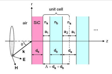
We proposed a potential coherent thermal emission source based on a
multilayer structure made of a polar material and a one-dimensional
(1-D) PC in the half plane, as shown in Fig. 1 [1]. The unit cell of
a 1-D PC is a binary layer consisting of a dielectric (type a)
on both sides of a dielectric (type b) with a total thickness
(lattice constant)
L
= da + db, where da
= a1 + a2. SiC is chosen
as the polar material to have coherent emission in the mid-infrared
region. The unit cell of the PC The surface termination is
determined by the thickness of the dielectric (a1)
located at the surface of the PC.
|
 |
|
Figure 1. Schematic of the multilayer structure made of a
SiC layer coated on a semi-infinite 1-D PC. |
By examining the conditions that cause a large emission in a narrow
spectral range either into a well-defined direction or towards the
whole hemisphere isotropically, a regime map (refer to Fig. 2a) is
developed to distinguish the emissivity enhancement due to three
different mechanisms: (i) the excitation of surface waves, (ii)
cavity resonance mode, and (iii) the Brewster mode [2].
Here,
na=2.4 nb=1.5, and
L=3.0
mm
(da=db).
Figure
2b depicts the contour plot of the emissivity as a function of the
wavelength and emission angle for p polarization.
The
thickness of SiC is set to be 1.45
mm.
For
p
polarization, as an example, large values of the emissivity are
found in Regions I and II, which are due to the excitation of the
surface waves and cavity resonance mode, respectively. Besides
Regions I and II, enhancement of emission is also found in the
wavelengths less than 10.4
mm
for a wide range of the emission angles, marked as Region III. The
emissivity enhancement in Region III is recognized as the Brewster
mode because it occurs only for p polarization. On the other
hand, the excitation of surface waves and cavity resonance mode can
occur for both p and s polarizations.
 |
 |
|
Figure 2. Identification of the important regimes where
the radiative properties are dominated by different
mechanisms. (a) The regime map in
l-q
space. (b) Contour plot of the spectral-directional
emissivity of the SiC-PC structure for p
polarization. |
The proposed planar structure involves
only dielectric films, which can be fabricated with available vacuum
deposition techniques. Future research is needed to measure the
spectral-directional emissivity from the proposed SiC-PC structure.
Physical or chemical vapor deposition techniques will be used to
grown periodic layers on a suitable substrate, such as ZnSe or MgO.
The refractive index of ZnSe or ZnS is near 2.4 and that of KBr or
MgO is near 1.5. In order to explore coherent emission at shorter
wavelength, other polar materials, such as boron carbide (BC), boron
nitride (BN), and fused silica (SiO2), can be used in
place of SiC. The effect of surface wave and localization can be
further studied by using metallic films, such as tungsten (W),
tantalum (Ta), and vanadium (V). Furthermore, Au or Ag films can be
used to tune the spontaneous emission in the visible region.
Additional PC layers can be formed in front of the SiC and other
absorbing films to tune the emission characteristics. The
theoretical aspect of this research will focus on the understanding
of surface waves, plasmon and phonon polaritons, cavity resonance,
and photon localization on the optical and radiative properties of
nanostructured materials. This research will have a strong impact on
the development of thermophotovoltaic devices.
Publications
[1] Lee, B.J., Fu, C.J., and Zhang, Z.M., 2005, “Coherent
Thermal Emission from One-dimensional Photonic Crystals,” Applied
Physics Letters, 87, 071904-1/3. [selected for the August 22, 2005 issue of
Virtual Journal of Nanoscale Science & Technology]
[2] Lee, B.J., and Zhang, Z.M., 2005, “Coherent Thermal Emission
from Modified Periodic Multilayer Structures,” to be presented at
the International Mechanical Engineering Congress and Exposition,
November 5-11, 2005, Orlando, FL.
Go to TOP